Clock Controller Design
Published:
This post is Part 3 in a three part series on our design of a USB powered Nixie Tube Clock display.
Part 1 discusses the characterization of Nixie tubes.
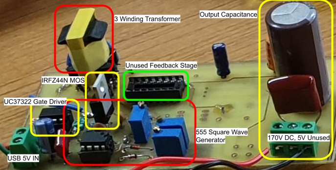
Part 2 discusses the design of the power supply that steps up 5V to 170V.
Controller Board Overview
The controller board a.k.a the USB bridge circuit is responsible for taking in timing information via USB from the host computer and displaying it, through the means of electrically isolated control signals, onto the front end display module consisting of 6 Nixie Tubes.
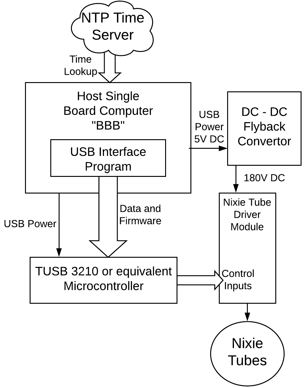
The flow of information and power is illustrated in the above block diagram. From the above block diagram, Nixie Tube Driver Module, Micro-controller and the Nixie Tubes are all part of the controller board. The details of these and some of their sub-components are illustrated next.
USB Controller Circuit
The most interesting component of the controller board is the USB micro-controller circuit. The host computer, which could be a single board computer for portability and compactness, is connected to the USB controller. After which the host side USB interface program first uploads the firmware onto the controller and then streams time information data to it. The firmware and host side program software was written with help from our advisor Prof. Mukul Chandorkar and is available here.
Two alternatives were considered for the USB controller circuit - the TUSB3210 and the FT232R chip. Our initial preference leaned towards the the FT232 from the desire for greater simplicity. Some problems with timing that could not be precisely controlled lead to us picking the TUSB3210 RAM based micro-controller. The details of these problems could be quite relevant to some other work and are available in our project report. To use the TUSB3210 controller in the USB connection circuit, some additional circuitry like its own power supply and some resetting circuitry were also needed. The details of these elements are also present in our project report.
An interesting question that needed to be answered was - What part of the processing should occur on the embedded controller and what parts should be done by the host computer? We pushed all the time keeping and computation onto the host computer leaving the USB controller with only the burden of two things.
(1) Translating the digits of time being streamed from the host to control signals that the display front end can understand and
(2) Using the control signals to multiplex between the various tubes in such a way that only a single tube is turned on at a time. This is required since the power available from the USB power source is, in principle, enough to light up only a single tube as discussed in part 1.
Optocoupler isolation and Control Signals
The GPIO pins on the microcontroller are responsible for the control signals that display the time on the Nixie Tubes. The design is configured in a manner that there are 10 control signals. The breakdown being - 6 signals for selection among the 6 tubes and 4 signals for digit selection among the digits 0-9 using a Binary Coded Decimal (BCD) code. In a more optimized design, the 6 tube selection signals could be replaced by 3 control signals and a decoder chip.
While designing the USB controller circuit described in the previous section, we thought that the 10mA or so of current required to turn the internal LEDs of the optocouplers on would be available from the GPIO pins of the controller itself. This assumption was based on a faulty reading of the somewhat unclear data sheet of the TUSB3210 controller. Since sufficient current could not be sourced from the controller directly, there had to be a current amplification stage sitting between the optocoupler input port (which is essentially an LED) and the signals being received from the GPIO pins.
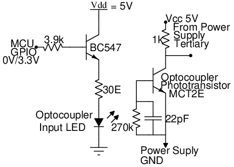
The current amplifier stage is essentially BJTs configured as switches which turn on when there is a small current going into the base of the transistors. The base current requirement is small enough that the GPIO pins from the TUSB controller can provide it. The complete arrangement for a single control signal is described in the above image. When the MCU GPIO signal is high, the BC547 transistor turns on which in turn switches on the IR LED at the input port of the optocoupler. Once the input LED is on, it excites the photo-sensitive base of the output photo-transistor which turns the transistor on. In the configuration available to us only the collector terminal of the output transistor is available to us.
As shown in the above circuit diagram, this would lead to the output signal being 5V high when the photo-transistor if off, and low when the photo-transistor is on. This is a problem since the photo-transistor needs to be turned on really hard for the output taken at the collector terminal of the transistor to be low enough for the subsequent electronic stage (which is the display front end) to recognize it as off. This forced us to pick a very low resistance value for the optocoupler input LED. As seen in the above diagram this value is 30 Ω. With such a low series resistance, the current pushed through the LED is high at about 30mA. This also reduces the life of the input LED significantly. We found ourselves replacing the optocoupler ICs quite often during testing. The only possible solutions to this problem seem to be either to look for an optocoupler IC that uses a very sensitive photo-transistor or to somehow change the sensitivity of the electronics following the output of the optocoupler to have a very high threshold for the on state, close to the high logic level of 5V DC.
The Display Front End
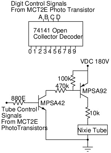
The display front end is where the previously mentioned 10 control signals get utilized. Four of these signals, marked A-D in the above diagram, are responsible for digit selection via the 74141 open collector decoder IC and the other six are for making a single Nixie tube light up at a time, that is to implement time multiplexing.
Multiplexing and Tube control
Six control signals are dedicated to selecting which tube turns on at any given time. The sequential turning off and on of tubes is implemented using a pair of BJT transistors as shown in the lower half of the above image. The arrangement of the pair of transistors is a variant of the darlington pair arrangement called the Sziklai Darlington Transistor Configuration and is described here. The configuration uses a high voltage NPN (MPSA42) and a high voltage PNP (MPSA92) transistor to effectively achieve stronger current amplification than a single BJT switch.
In this configuration, the Nixie tube would turn on when its corresponding NPN transistor (MPSA42 BJT) is on. To the outside circuit, the BJT pair simply appears as a highly sensitive NPN transistor since when the outer NPN transistor turns on, there is a sufficient base current coming out of the base current of the inner MPSA92 PNP transistor. This allows current to flow through the Nixie tube which turns it on.
Due to the high sensitivity of the transistor pair, the threshold for the low logic level comes out to be quite low. As described in the previous section, this leads to requirements on the optocoupler. The optocoupler input LEDs have to be turned on quite strongly so that the its corresponding output phototransistor turns on strongly and gives a ‘low enough’ (about 0.3V in this case) logic low voltage level.
Looking at the broader design of the optocoupler transmitting the control signal to the high voltage side, we identify a somewhat serious problem with the described design. The problem being that if we consider the default state of the optocoupler input LED to be off, then this means that the default state of the output phototransistor for each signal is off and its output is therefore high, this in turn means that the default state of any Nixie tube is on. Since we wish to turn on a single Nixie tube at a time (the goal of multiplexing), this means that 5 out of 6 optocoupler input LEDs need to be turned on strongly for 5 unselected tubes to be off at all times. Signal inversion at the high voltage end or some other changes in the design can solve this problem and can reduce wear on the optocoupler LEDs in addition to decreasing power usage significantly on the low voltage USB side.
Digit Selection using the 74141 IC
Each Nixie Tube has a total of twelve pins, one Anode and eleven cathodes corresponding to the digits 0-9 and a decimal point. Barring the decimal point, there needs to be a mechanism to choose between the 10 digits at any given instant. An off the shelf solution is available for the same in the form of the SN74141 TTL IC. The differences between the 74141 and a regular BCD decoder such as the 7442 are the presence of open collector outputs with Zener Diode Clamping and the use of high voltage rating transistors at the outputs in case of the 74141 which are absent in the 7442. This is crucial for the Nixie tube application since a large voltage could appear on the cathodes corresponding to digits that aren’t turned on for a tube that is glowing.
For the 74141 IC the low level input voltage is allowed to be up to 0.8V. This requirement is not as strenuous as the one for turning off a Nixie tube but the problem of turning on the input LED of an optocoupler strongly to achieve a low logic level at the phototransistor output still holds true but the issue with the default value of a phototransistor being on is not a problem since the required input signals onto the pins A-D are a mix of high and low levels.
The SN74141 IC is not the ideal way to implement digit selection for the Nixie tubes since the chip has now been discontinued. Further we found the 74141 to be quite unreliable with numerous failures during the testing process. A reproducible and more reliable approach would be to use high voltage shift registers (a.k.a serial to parallel convertors). In this design exercise that creates a Nixie tube display, Dave from the EEVBlog recommends using the HV5622 or other similar ICs.
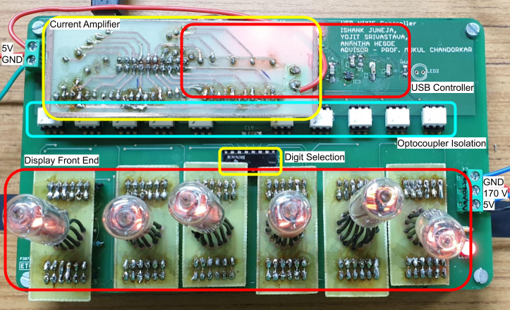
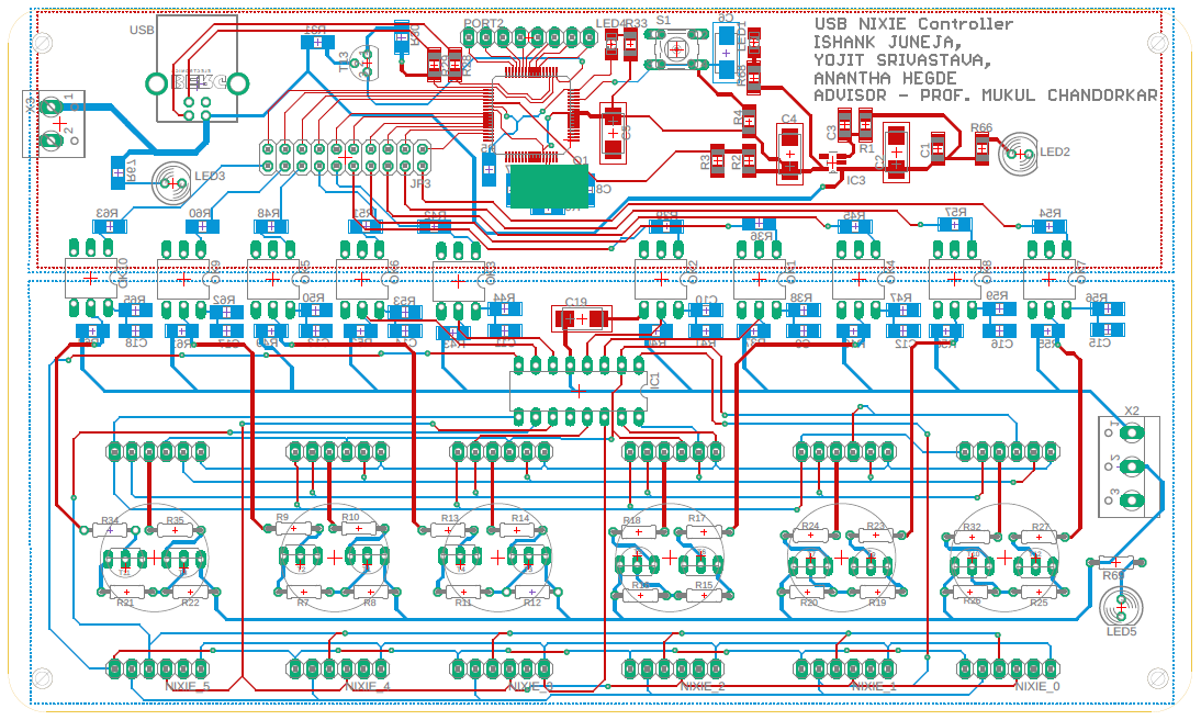
The Complete Board View
The final board design is quite elegant and symmetrical in our opinion.
This project was completed in partial fulfilment of the requirements for EE 344: Electronic Design Lab at IITB
A more detailed description of the project along with schematics can be found in our project report
A demonstration of our project can be found here