Power Supply Design
Published:
This post is Part 2 in a three part series on our design of a USB powered Nixie Tube Clock display.
Part 1 discusses the characterization of Nixie tubes.
Part 3 describes the design of a circuit which controls the display using isolated control signals.
This work on the design of the power supply was spearheaded by Anantha Hegde and Yojit Srivastava. ***
Introduction
This page is about the design of the power supply module from our USB powered Nixie Tube clock display project. Since the USB source voltage is 5V DC and the operating voltage of the Nixie Tube display units is close to 180V DC, we needed to design a power supply capable of achieving this voltage step up. DC-DC power conversion and a large difference between input and output voltage difference mandated a switched mode (SMPS) isolated power supply.
Despite the high output voltage level required, the convertor still operates in the low power regime (about 2.5 W as explained in part 1). This made the Flyback convertor topology ideal for our purpose.
Related Existing Solutions - Survey
Before we describe the solution we ended up implementing to reach the described end goal, let us look at some of the other solutions we considered prior to it. On scouring the web we found a few solutions that matched our requirement closely. Most of these solutions had an input operating voltage of 9V-12V. Perhaps this restriction of a slightly higher than available input voltage has something to do with most batteries (Lead Acid for example) having a terminal voltage in that range.
Single IC Based solutions
TNY-278
Our first attempt at a Power Supply was with the TNY-278 IC by Power Integrations. This was our starting point since this chip was available in our project advisors lab. The TNY-278 is a switching IC which has a typical application of a step down convertor in a flyback like type topology (can be seen in linked data sheet). Our intention was to reverse the input and output ports of its typical application circuit to use the chip in a step up convertor. However, we soon realized that the usage of such a topology with a 5V input voltage would not be possible since the internal circuitry of the TNY-278 makes any voltage below 5.85V unusable. However, we never showed that the operation of the TNY-278 IC could be mirrored in the first place. We simply rejected the idea since it would certainly not work with a 5V input.
LM3488
Quite close to the start of our work we came across this well documented project. The linked project describes the design of a Flyback convertor that steps up 5-12V to 180V. On the surface of it, this seemed like the end to our search. In fact we even went ahead and got a circuit board printed for this circuit. The schematic and the board view are pictured below.
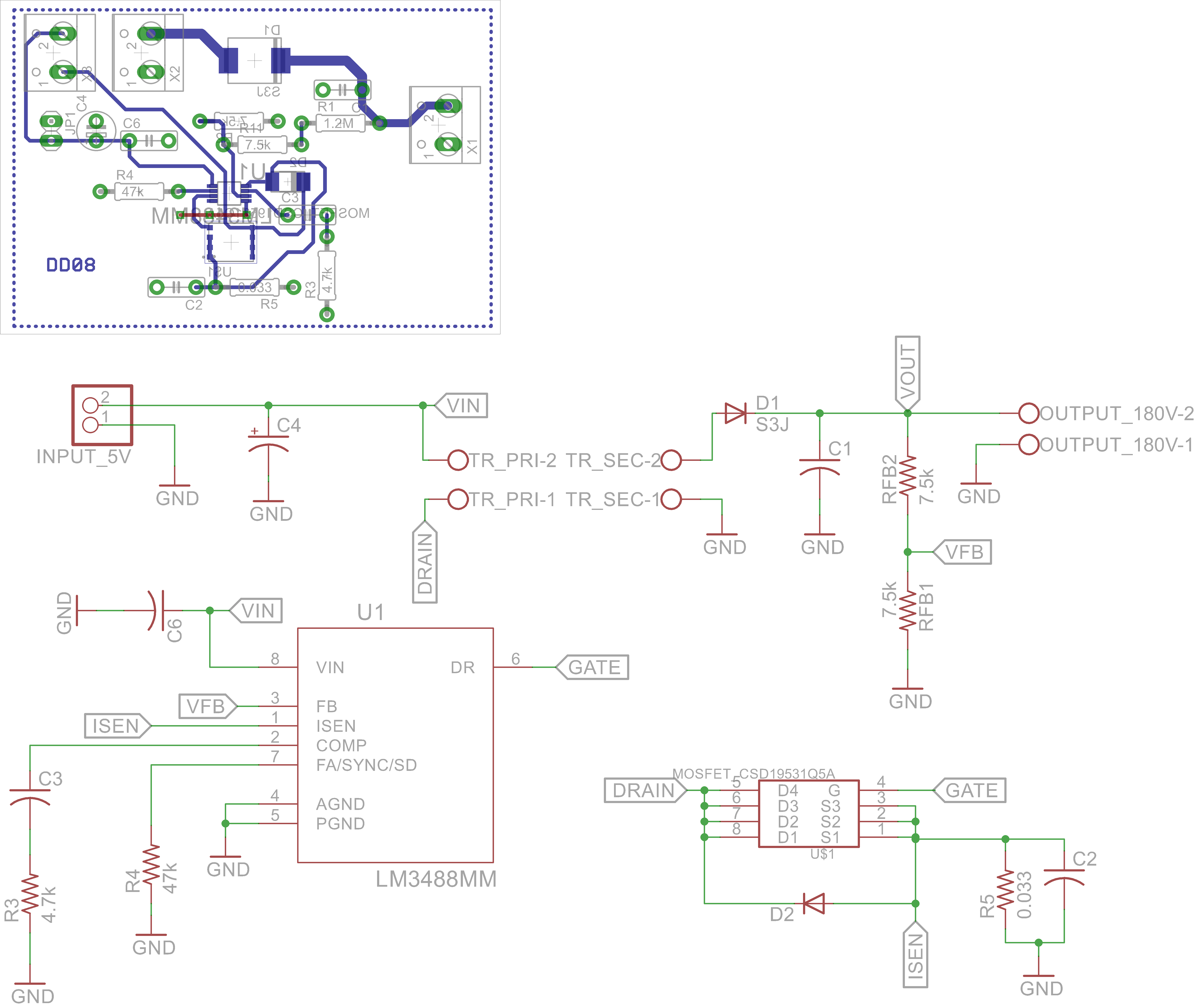
The circuit is essentially a Flyback topology built around the LM 3488 IC. The LM 3488 is the complete package as far as a switched power supply (SMPS) is concerned since it has voltage feedback from the output (FB pin), MOSFET gate drive (DR) and the switching frequency set (FA/SYNC/SD) all built into a single package. However, the design in the linked project destroyed the isolation obtained from the transformer of the Flyback convertor by sending in a direct voltage feedback from the HV side to the LV side without optocoupler isolation in between.
Since this was a critical design flaw for our application (the need for isolation is described in the next section) we decided to look for our own solutions starting from scratch. So, next began the phase of designing switched mode convertors from scratch using discrete components rather than packaged IC solutions.
Discrete Components Based Solutions
Initial Design Process - Boost Convertor

We started off the design process by putting together a Boost convertor. The question of whether a MOS or a BJT should be used as the electronic switch in our design was asked. Compared to a MOSFET, a BJT has a slower transient response and higher losses due to a continuous base current and a higher voltage drop across the Collector - Emitter junction.
Our choice of MOSFET was the IRFZ44N. This MOSFET fell well within the voltage and current ranges in which we would eventually want to operate our Flyback convertor switch. We tried switching this MOSFET using a switching frequency of 100KHz.
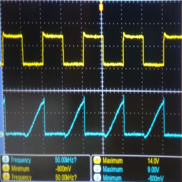
Initially when this was tried with the switching signal, a square wave of 100KHz, was provided directly to the date drive (pin) of the MOSFET. Soon we realized that the analog function generator (AFG), is unable to provide sufficient current for the MOSFET to be able to switch fast enough. This leads to the faulty on-off waveform in blue in the above figure. This calls for the need of a separate gate-drive stage which takes in a switching signal without imposing a load on it and echoes the same signal to a high current capacity gate-drive line.
Our initial design used the HCPL-3120 as the higher current capacity gate drive and the SG3542 as the function generator. The HCPL chip is a standard gate drive chip and the SG3542 provides an easy interface to set the frequency and duty cycle independently. After making these changes to the design of our Boost convertor, we obtain the below cleaner waveforms. There continue to be some large stray transients that need to be done away with before use in a real convertor. After making some more changes, tweaking the values and ratings of some circuit components we ended up making the Boost convertor work. The details are available in our project report.
Flyback convertor and transformer design
Rather than the choice of a Flyback convertor, a non-isolated Boost convertor with a voltage boost from 5V to 180V could have been used. However, since the power and data source is a single USB port on a computer, it is crucial that we keep the low voltage (LV) and high voltage (HV) sides electrically isolated from each other. The only way to do this would be to choose an isolated convertor.
Further, an isolated convertor like the Flyback has the advantage of being able to utilise the turns ratio of its transformer as the voltage step up component. The problem of a high step up of $\frac{180}{5} = 36$ times using a non-isolated Boost convertor can be illustrated by comparing the input to output transfer functions of the Boost and the Flyback convertors.
The Boost convertor has the input $V_i$ to output $V_o$ transfer function of \[V_o = \frac{V_i}{1-D}.\] Where $D$ is the duty cycle (or the fraction time spent on). So for a step up of $36$ times an unsustainable $D$ of $\frac{35}{36}$ will be required. However, now we can consider the Flyback convertor topology used.

Due to the transformer present in the circuit, the transfer function is given by, \[V_o = \frac{N_2}{N_1} \frac{D}{1-D} V_i.\] Where $\frac{N_2}{N_1}$ is the turns ratio of the transformer in question. With a reasonably large turns ratio, little of the step up burden falls on the $D$ term thereby making for a reasonable duty cycle.
The transformer was the central component for the successful design of the flyback convertor. The design of the transformer was undertaken for a switching frequency of 100KHz. As a fun design exercise, we decided to create a transformer from scratch instead of outsourcing the task to a workshop. With help from research assistants from the Applied Power Electronics Lab (APEL) we managed to achieve our goal.
This transformer needed to have one input winding for the 5V USB power source, and two output windings. One output winding would correspond to the 180V output to power the Nixie tubes. An additional isolated 5V power output was required by us to power the silicon on the High Voltage side (see part 3 for details). After completion, the specs of the transformer can be found in our report. To complete the flyback convertor, the design we came up with initially was as follows,
Here the components on the HV side remain similar to the earlier boost convertor. The key difference being that they are rated for suitably high voltages. The switching signal of a 100KHz square wave is provided to the MOSFET directly from a 555 timer. The duty cycle (which controls $D$) and the frequency of the 555 timer can be controlled using individual potentiometers in this design.
A problem with this design is similar to the problem with driving a MOSFET gate with an analog function generator. The current that can be drawn from the output of the 555 timer is limited since the 555 chip is designed as a timer or perhaps a signal generator. In the design of the power supply, this problem manifests itself in the large switching losses that arise within the MOSFET switch. As can be seen in the figure depicting the switching of the IRFZ44N MOSFET when driven through an AFG, poor switching quality leads to a longer transition period between the on and off states. This causes significantly more heat loss in accordance with Joule’s law of heating.
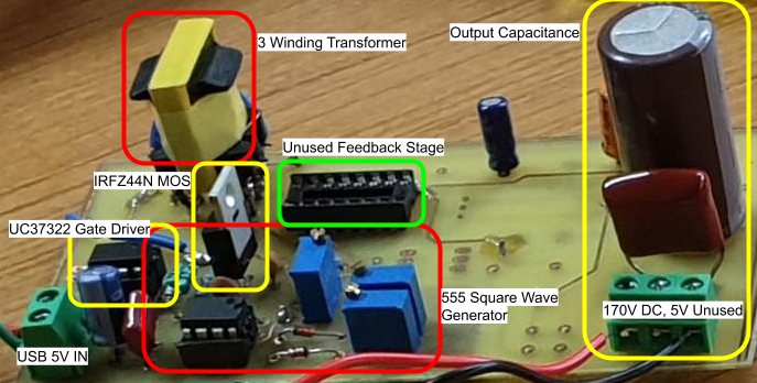
This problem was solved by sandwiching the UC37322 gate driver between the 555 timer and the MOSFET gate. This allowed for a much better switching waveform thereby reducing the heating and energy loss from the IRFZ44N significantly. The last problem that remains to be solved is that of over voltage at the output side under no load conditions. This problem must be solved since in the absence of control on the output, the voltage would go increasing indefinitely damaging the circuit components.
Feedback Control of Output Voltage
If the switching action in a boost convertor is turned off, the output voltage ceases to build up. In such a case in the absence of any output load, the output voltage would not decrease or increase but rather remain constant. This situation may not be ideal but is still better than the voltage going on increasing indefinitely. The easiest way to shut off switching in our design would be to use the reset pin on the 555 timer generating the switching waveform. Another factor is that we must keep the reset signal of the 555 timer on the LV side and the voltage feedback signal on the HV side isolated from each other. This is achieved using opto-coupler signal isolation using an MCT2E between the two sides.
The details of the feedback mechanism can be found in the lower half of the below schematic. The mechanism for how this feedback works is quite interesting. An LM324 opamp is configured as a comparator with the regulated 5V power supply intended for HV side silicon connected to the ‘+’ terminal of the comparator and a voltage divided version of the 180V (called VFB) output connected to the ‘-‘ terminal of the comparator. When VFB becomes too large, the output of the comparator turns off, thereby turning the output of the MCT2E phototransistor off which in turn resets the 555 timer output through the active low RESET pin. This RESET state remains the situation until the output voltage at the HV side drops below a certain threshold. Once the voltage drops by enough the phototransistor turns on again starting the switching action and the voltage gain. In the absence of a real load, this on-off procedure would continue cyclically.
More details about the circuit board layout with SMPS best practices and details about the creating tertiary winding of the transformer can be found in our project report.
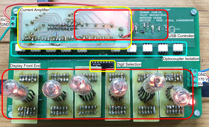
It would be appropriate to add here that though the feedback mechanism was tested on our earlier breadboard based design, it did not function correctly when placed within the final circuit board. Primarily, this had to do with the additional 5V power source from the tertiary winding of our transformer not functioning correctly. Hence the unused feedback stage is seen in the image at the start. Importantly, this makes the final power supply unsafe to use without a load connected.
Mr. Joginder Yadav, RA Machines Lab, IIT Bombay provided immense help for the design of the power supply and other modules of this project
This project was completed in partial fulfilment of the requirements for EE 344: Electronic Design Lab at IITB
A more detailed description of the project along with schematics can be found in our project report
A demonstration of our project can be found here